CMOS Digital Integrated Circuit Design
Duration: 9h 20m | .MP4 1280x720, 30 fps(r) | AAC, 44100 Hz, 2ch | 5.94 GB
Genre: eLearning | Language: English
Duration: 9h 20m | .MP4 1280x720, 30 fps(r) | AAC, 44100 Hz, 2ch | 5.94 GB
Genre: eLearning | Language: English
Introduction to VLSI Digital Integrated Circuit Design in NMOS and CMOS
What you'll learn
NMOS Circuit Design
CMOS Circuit Design
Device Physics
Static Logic
Digital Design
Electric Electronic Design Automation (EDA)
Circuit Layout
Requirements
Enthusiasm
Description
In this course we cover the basics of NMOS and CMOS Digital Integrated Circuit Design. If you are looking for an introduction to this subject then this is the course for you.
We start with a look at some device physics. This will allow us to be introduced to some terminology and will set the foundations for the rest of the course. We then move onto device fabrication and layout which will be covered more extensively when we look at designing and simulating our circuits in an Electronic Design Automation tool (EDA) called Electric which you can download for free and give it a go yourself.
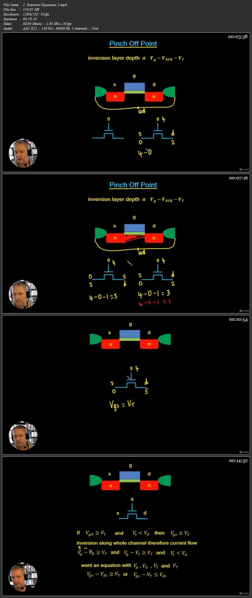
We then look at deriving some equations that allow us to understand and use the MOSFET (Metal Oxide Field Effect Transistors) transistors to build useful digital logic circuits. We then cement our understanding of the 4 device types depletion and enhancement nmos and pmos devices using a simple simulation which I built myself which gives a good intuitive understanding of the MOSFET.
Then we move onto simple pass transistor circuits which allow us to get used to the transistor equations and will also help us with an understanding of dynamic logic.
We cover the Inverter (NOT gate) in detail as we will use this as the building block for many future circuits.
We then come to the section on NMOS circuit design where we design simple building blocks such as NOR and NAND gates and other simple gates and random combinational logic culminating in the full adder circuit. The next section covers CMOS circuit design and again we work through the design of the basic logic building blocks culminating in a full adder circuit.
The final section covers the EDA tool called electric in which we design and layout our CMOS circuits finishing off with a full adder circuit.
I have spent 7 years after graduation as an Integrated Circuit Designer with a world leading design house. I also have spent 4 years with a company with it's own wafer fabrication plant which allowed me to not only design the integrated circuits (chips) but also follow the production process and to work through the full characterisation then implementation of the chip into a customers system . So I have worked through several end to end life cycles of chips that are out there and working now.
Who this course is for:
Absolute Beginner
More Info


