

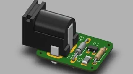
PCB Design Crash Course: 3D Package & Board Design Approach

PCB Design Crash Course: 3D Package & Board Design Approach
MP4 | Video: h264, 1280x720 | Audio: AAC, 44.1 KHz, 2 Ch
Genre: eLearning | Language: English + srt | Duration: 10 lectures (3h 31m) | Size: 1.93 GB
MP4 | Video: h264, 1280x720 | Audio: AAC, 44.1 KHz, 2 Ch
Genre: eLearning | Language: English + srt | Duration: 10 lectures (3h 31m) | Size: 1.93 GB
Learn Eagle PCB Design from Schematic design to Board Design in 3D view
What you'll learn:
Printed Circuit Board Layout Design
Circuit Design and Analysis
Basic Electronics
Electronic components and instruments
Board Design and Fabrication
Schematic design: Entry to expert level
Footprint creation: All packages including 3D modelling
Board Design: Single sided, Double sided and multilayer
Constraint manager settings
Double sided Board Design
Multilayer Board Design
Via management
Via creation and application
Blind via, Berried via and Through hole via
Deign Rules Checking (DRC Errors)
Gerber creation
Gerber analysis and improvements
PCB Manufacturing overview
Requirements
Basic Electronics knowledge
Diploma (Electronics or Electrical)
Bachelors in Electronics and Electrical
Master degree in Electronics and Electrical
Post graduate in Electronics and communication engineering
BE in Electronics and Communication
PCB Manufacturer
Bachelor of Engineering in Electrical and Electronics
BSc in Electronics
MSc in Electronics
MS in Electronics
Post graduate in Electronics and communication
Description
PCB Design in Eagle cad tool and electronics circuit are basements for all type of electronics products. PCBs are derived from the analog and digital circuits which are prepared according to the application required. Printed circuit boards are the main pillars of the Electronics world. Every Electronics products has PCB inside it, from consumer gadgets like computers, smart phones and gaming consoles to industry and even high-tech products.
Required eligibility:
Diploma in Electrical or Electronics & Communication.
BE/BTech. in Electrical or Electronics & Communication.
BSc/MSc in Electronics & Communication.
ME/MTech. (E&CE) in Communication.
PCB Design Course Content is given below in brief:
Schematic Design:
Basic Electronics theory.
Basics of Circuit designing.
Schematic design preparation.
Schematic part editing and creation.
Net list and Net class creation.
Bill Of Material generation (BOM).
Electrical Rule Checking.
Footprint Creation:
Through hole footprint creation.
Surface Mount Device footprint creation.
BGA/PGA footprint creation.
Board Designing:
Board size and shape creation.
Component placements.
PCB Routing: 2 to 16 Layer routing.
Plane creation.
Design rule checking.
Gerber generation.
Skills you gain after the course completion:
Basic Electronics and Electronic components expertise.
Circuit Designing (Power management circuit designing)
Circuit Simulation for best understanding of the subject.
Tools/Software Expertise.
Basic design module practice up to 4-Layers.
Advanced design module practice up to 16-Layers.
Design expertise:
o Assignments consists single and double sided PCB.
o Assignments consists 2-Layers to 16-Layers design.
Library Module:
o Symbol and Footprint design for all types of packages.
High speed placements & routing techniques.
Power integrity and Signal Integrity analysis.
Design for Manufacturing, Testing and Fabrication expertise.
Gerber generation and editing.
Benefits of choosing PCB Design Course:
Strong hold in basic electronics.
Circuit Design capability.
Circuit analysis & ERC.
Components knowledge.
Power Supply designing.
Power Integrity Analysis.
Multiple PCB-CAD tool expertise.
Expert in library creation.
Multi-layer PCB designing.
Signal Integrity Analysis.
High speed PCB designing.
Gerber creation & editing.
Who this course is for
Diploma in electronics
Hardware designers
PCB manufacturer
Electronic Components engineer
PCB design and developer
Circuit designers
Embedded engineers
Beginners interested in development of PCB