


Vsd - Design Process Linkages And Components In Cmos Process
Vsd - Design Process Linkages And Components In Cmos Process
Last updated 8/2024
MP4 | Video: h264, 1280x720 | Audio: AAC, 44.1 KHz
Language: English | Size: 332.94 MB | Duration: 1h 7m
Last updated 8/2024
MP4 | Video: h264, 1280x720 | Audio: AAC, 44.1 KHz
Language: English | Size: 332.94 MB | Duration: 1h 7m
Ever wondered what happens post SoC design? And how it happens?
What you'll learn
Industrial Analog design
Industrial CMOS process
Issues and challenges in deep sub-micron technology
Design analog components in standard CMOS process
Requirements
Physical design and custom layout knowledge is nice to have
Should have knowledge on basic digital design and logic gates
Nice to have awareness about VLSI design basics and SoC design
Description
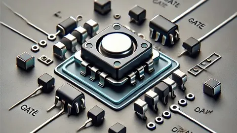
HS Jatana, with a distinguished career spanning over three decades in the VLSI industry, brings a wealth of experience and expertise to this course. Having worked at Rockwell Semiconductor in the USA, he has made significant contributions to process development and integration, device testing and characterization, and IC design. His hands-on experience in these critical areas has shaped his deep understanding of the intricacies of semiconductor technology. Currently, as the Group Head at the Semiconductor Laboratory (SCL), Jatana continues to lead and innovate in the field.This course offers a comprehensive overview of basic analog and digital design flows from a manufacturing perspective, with a particular focus on the nuances that practitioners encounter in real-world applications. Key topics include Process Design Kits (PDKs), Pcells, and detailed insights into the 180nm technology node, including cross-sectional views and practical examples.The course also delves into the various components available in a standard CMOS process. It explains the basic structures of different elements and how they are realized in the manufacturing process. Special emphasis is placed on passive components, which are crucial in any mixed-signal design. Participants will explore the features, advantages, and disadvantages of these passive elements, gaining a thorough understanding of their role in modern VLSI design.
Overview
Section 1: Introduction
Lecture 1 Introduction
Section 2: Steps involved from design to manufacturing
Lecture 2 Analog and digital design flow
Lecture 3 Introduction to real 4-metal PDK
Lecture 4 General cross-section in 180nm tech node and PDK's
Lecture 5 PDK description, technology file and Pcells
Section 3: Devices and Model Files
Lecture 6 Model Files
Lecture 7 Legal Devices - MOSFETs Diodes Resistors
Lecture 8 Bipolar Devices And Capacitors
Lecture 9 NMOS Parameters And Standard Cell Library
Lecture 10 Memory IP And IO Library
Lecture 11 Design Rule Checks
VLSI design fresher who is curious for design manufacutring processes,Experienced SoC design professionals who is curious to know what happens inside CMOS manufacturing process